(China (Mainland))

Product Summary
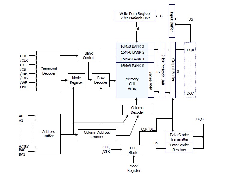
The H5DU5162ETR-E3C is a 512Mb DDR SDRAM. The H5DU5162ETR-E3C is ideally suited for the main memory applications which requires large memory density and high bandwidth. This H5DU5162ETR-E3C offers fully synchronous operations referenced to both rising and falling edges of the clock. While all addresses and control inputs are latched on the rising edges of the CK (falling edges of the /CK), Data, Data strobes and Write data masks inputs are sampled on both rising and falling edges of it. The data paths are internally pipelined and 2-bit prefetched to achieve very high bandwidth. All input and output voltage levels are compatible with SSTL_2.
Parametrics
H5DU5162ETR-E3C absolute maximum ratings: (1)Operating Temperature (Ambient)TA: 0 ~ 70 ℃; (2)Storage Temperature TSTG: -55 ~ 150 ℃; (3)Voltage on VDD relative to VSS VDD: -1.0 ~ 3.6 V; (4)Voltage on VDDQ relative to VSS VDDQ: -1.0 ~ 3.6 V; (5)Voltage on inputs relative to VSS VINPUT: -1.0 ~ 3.6 V; (6)Voltage on I/O pins relative to VSS VIO: -0.5 ~3.6 V; (7)Output Short Circuit Current IOS: 50 mA; (8)Soldering Temperature Time TSOLDER: 260 .10℃.Sec.
Features
H5DU5162ETR-E3C features: (1)VDD, VDDQ = 2.5V +/- 0.2V; (2)All inputs and outputs are compatible with SSTL_2 interface; (3)Fully differential clock inputs (CK, /CK)operation; (4)Double data rate interface; (5)Source synchronous - data transaction aligned to; (6)bidirectional data strobe (DQS); (7)x16 device has two bytewide data strobes (UDQS, LDQS)per each x8 I/O; (8)Data outputs on DQS edges when read (edged DQ)Data inputs on DQS centers when write (centered DQ); (9)On chip DLL align DQ and DQS transition with CK transition; (10)DM mask write data-in at the both rising and falling edges of the data strobe; (11)All addresses and control inputs except data, data strobes and data masks latched on the rising edges of the clock; (12)Programmable CAS latency 2/2.5 (DDR200, 266, 333), 3 (DDR400)and 4 (DDR500)supported; (13)Programmable burst length 2/4/8 with both sequential and interleave mode; (14)Internal four bank operations with single pulsed /RAS; (15)Auto refresh and self refresh supported; (16)tRAS lock out function supported; (17)8192 refresh cycles/64ms; (18)JEDEC standard 400mil 66pin TSOP-II with 0.65mm pin pitch.
Diagrams